 View all instruments of this unit
 Scanning Electron Microscope (FIB/ SEM) FEI (now Thermo Fisher) Helios Nanolab 660
Basic Information
| Name: | Scanning Electron Microscope (FIB/ SEM) | |
| Manufacturer: | FEI (now Thermo Fisher) | |
| Model: | Helios Nanolab 660 | |
| Facility: | Dresden Center for Nanoanalysis (DCN) |
|
| Partner: | Technische Universität Dresden (TUD) |
|
| Location: | Barkhausenbau, Room S81 | |
Short Description
Description
The FEI Helios Nanolab 660 is a state-of-the-art Ga-FIB/SEM tool with an electron image resolution of 0.9nm between 1kV and 30kV and a resolution of 1.5nm between 350V and 1kV. The resolution for ion imaging is 2.5nm at 30kV. The system features a wealth of detectors such as SE, BSE and SI chamber detectors and SE, BSE and low-loss BSE in-column detectors as well as STEM detectors for operation as a low-voltage STEM (BF, annular DF1-4 and a segmented HAADF).
The system also enables for ultra-low landing energy imaging with a freely adjustable beam deceleration option of up to 4kV.
The system is well equipped for focussed ion beam based sample modification using any of the 5 GIS systems for deposition of C, Pt or W and XeF2 for enhanced removal of material (Si and SiO2). It also features an experimental gas inlet for parallel local injection of a gas (air, O2) or in-situ low-voltage Ar-sputtering (currently not configured). It is furthermore equipped with the FEI EasyLift, the FEI micromanipulator which is fully integrated into the system.
In addition, the system has 7 electrical feed-throughs for in situ experiments (common ground), the possibility for 2 door-mounted Kleindiek manipulators (tips, grippers, rototip and electrical transport measurement). It is possible to reconfigure the system to 4 electrical contacts (2 Kleindiek, microscope stage and EasyLift). There is also a homebuilt heating stage available.
The system is ideally suited for low-voltage, high resolution SEM studies, TEM sample preparation, circuit modification, in situ experiments and much more.
Link to Further Details
Options of instrument usage
- This instrument can be used as an stand-alone device and is available for independent use. Please note possible requirements for access.
- This instrument can be used with the support of a supervising assistant.
- This instrument is used within a service or research collaboration.
Points of Contact
Access Requirements
Experience in FIB/SEM usage, preferably on FEI tools and/or training course and signing of user agreement. License required. Contact the DCN staff for further details.
Notes
Booking in chunks of 1h, maximum 1 day.
Images
| Preview | Description |
|---|---|
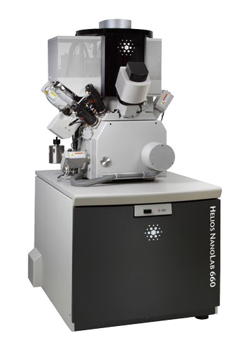
Source: © www.fei.com |
FIB/ SEM Helios NanoLab 660 |
Last Update
Last updated at: 27 October 2023 at 08:41:38