 View all instruments of this unit
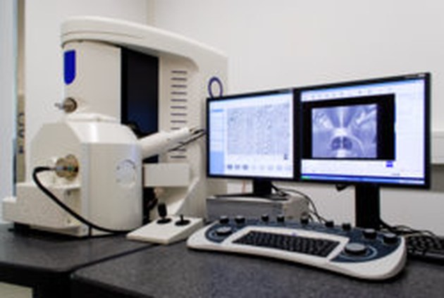
 Scanning Electron Microscope (SEM) Carl Zeiss Microscopy GmbH Zeiss EVO 10
Basic Information
| Name: | Scanning Electron Microscope (SEM) | |
| Manufacturer: | Carl Zeiss Microscopy GmbH | |
| Model: | Zeiss EVO 10 | |
| Facility: | Kleblabor | |
| Partner: | Technische Universität Dresden (TUD) |
|
Description
The scanning electron microscope (SEM) makes it possible to achieve a significantly higher magnification rate than a conventional light microscope by electron image formation. With this device, magnifications up to 200,000-fold are possible. Thus, insights into areas of the surface structure which are not possible with conventional means can be obtained. With the use of a micro-tensile module, the REM can show damage to tensile stresses, which may eventually lead to failure of the component. By means of the use of a vacuum diaphragm and thus the generation of a low vacuum in the sample chamber, plastics and nonmetals, which the electrons can not dissipate, can also be imaged very well.
Link to Further Details
Points of Contact
Associated Services
| Name | Preview | Actions |
|---|---|---|
| Microscopic material and material analysis / characterization of material surfaces |
Images
| Preview | Description |
|---|---|
|
REM Zeiss EVO 10 (Quelle: www.tu-dresden.de/bu/bauingenieurwesen/bauko/) |
Last Update
Last updated at: 26 September 2017 at 12:41:14