

 View all instruments of this unit
 Scanning Electron Microscope (SEM) JEOL GmbH JSM-6610LV
Basic Information
| Name: | Scanning Electron Microscope (SEM) | |
| Manufacturer: | JEOL GmbH | |
| Model: | JSM-6610LV | |
| Facility: | Competence Materials Characterization and Testing |

|
| Partner: | Fraunhofer Institute for Material and Beam Technology (IWS) |

|
Short Description
Analytical scanning electron microscope with "Low-Vacuum"
Description
- Equipment/ technical data
- Emission: tungsten cathode
- Acceleration voltage: 1 kV to 30 kV
- Resolution: 3 nm (30 kV), 15 nm (1 kV)
- Detectors: SE, BSE
- “Low-Vacuum”- operation for analysis of low conducting specimens
- Additional equipment: EDX-detector (Oxford Instruments)
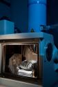
- Large specimen chamber suitable for specimen size up to 200 mm
- Methods
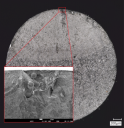
- Scanning electron micrographs of specimen surfaces
- Analysis of diverse structure specifications of metallic and non-metallic materials
- determination of chemical composition including light elements (B,C,N,O) with high local resolution
Options of instrument usage
- This instrument is used within a service or research collaboration.
Points of Contact
Prof. Dr. Martina Zimmermann
Web:
Phone:
+49 351 83391-3573
Notes
.
Associated Services
Images
| Preview | Description |
|---|---|
Source: Fraunhofer IWS |
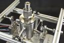
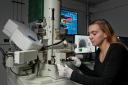
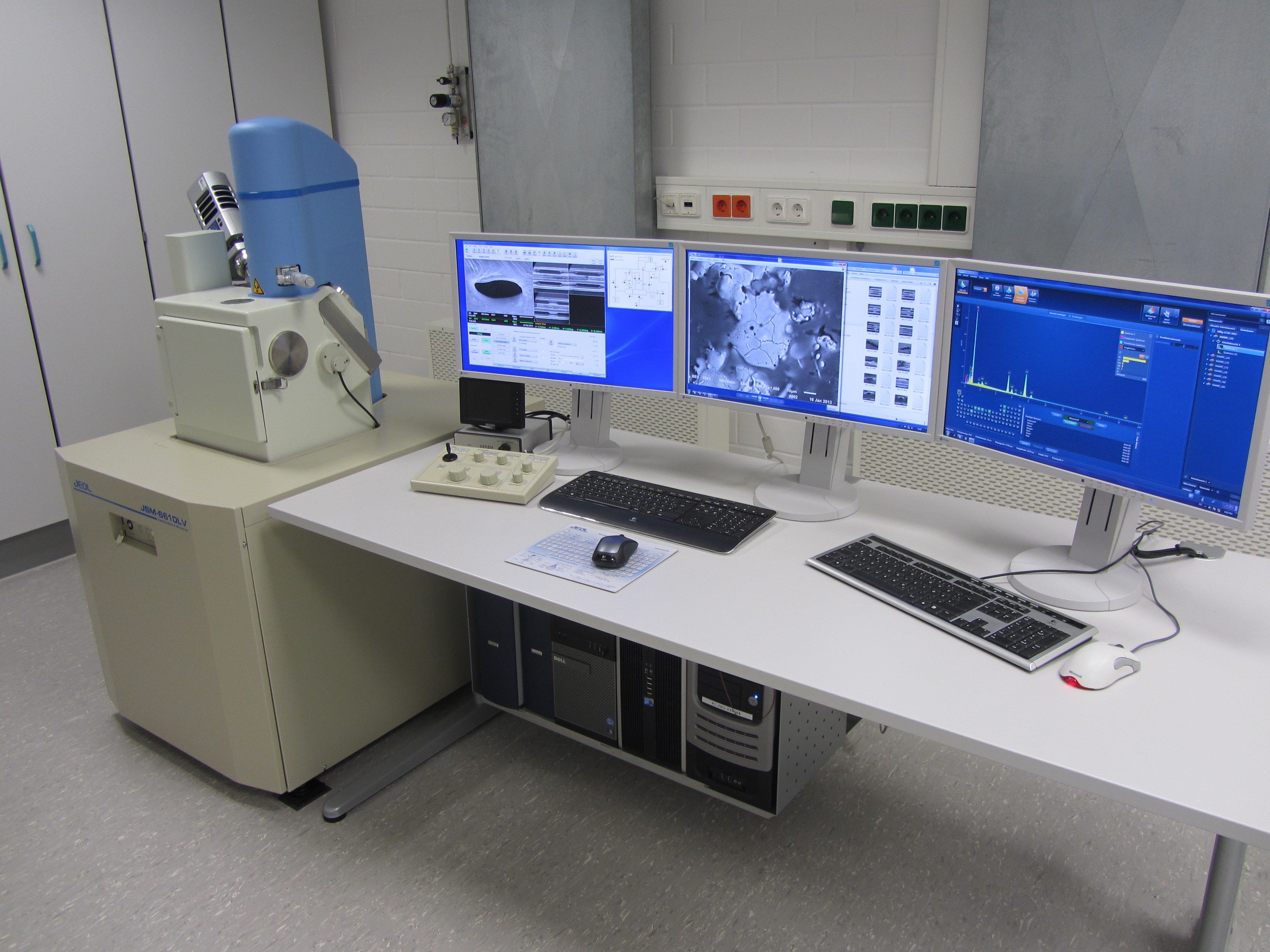
Analytical scanning electron microscope - JEOL JSM-6610 LV |
Last Update
Last updated at: 5 August 2019 at 10:16:43