 View all instruments of this unit
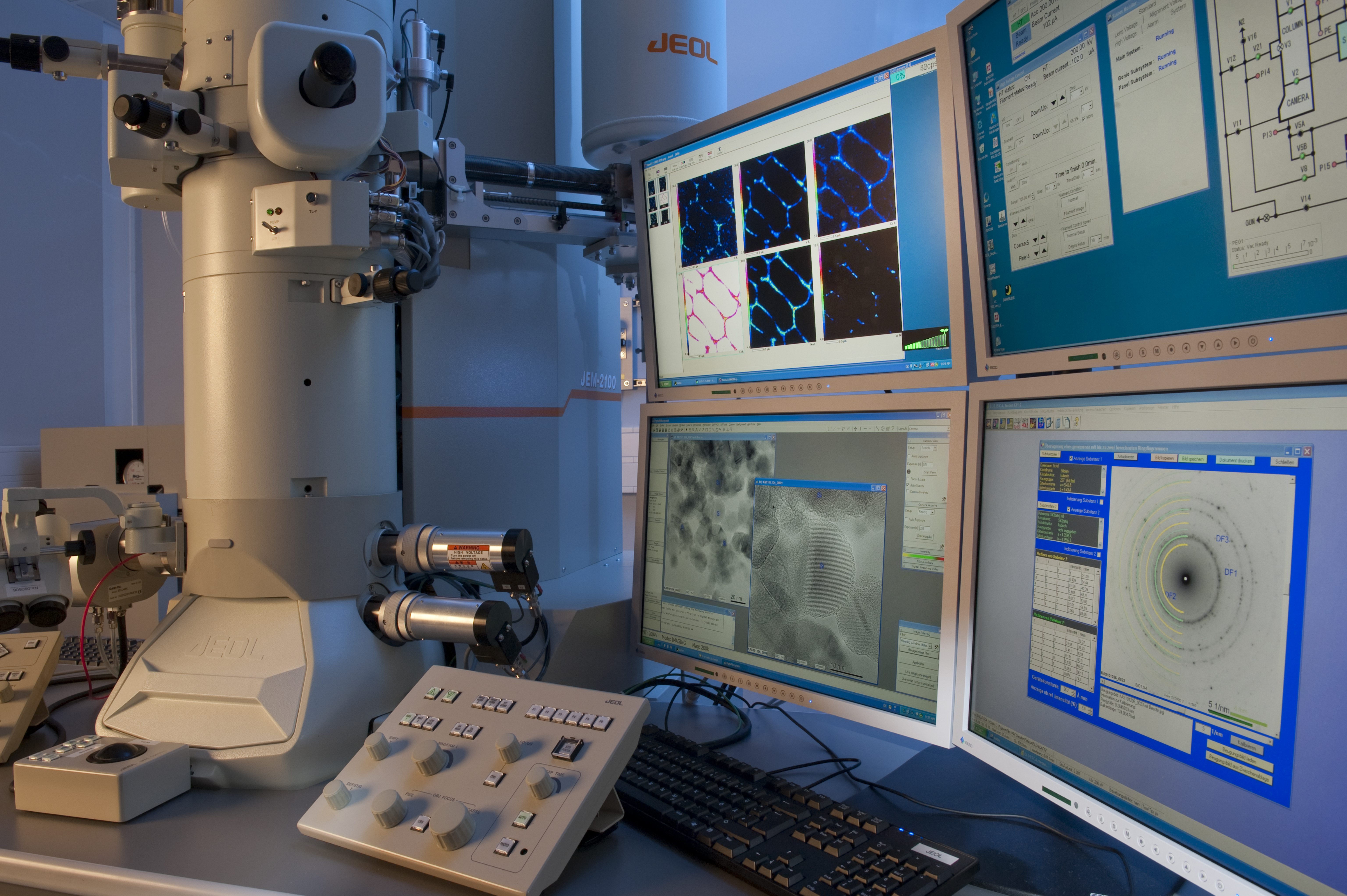
 Analytic transmission electron microscope 200 kV JEOL JEM-2100Plus
Basic Information
| Name: | Analytic transmission electron microscope 200 kV | |
| Manufacturer: | JEOL | |
| Model: | JEM-2100Plus | |
| Facility: | Competence Materials Characterization and Testing |

|
| Partner: | Fraunhofer Institute for Material and Beam Technology (IWS) |
|
Short Description
Analytic transmission electron microscope 200 kV- JEOL JEM-2100Plus
Description
- Equipment/ technical data
- Emission: LaB6-Cathode
- Acceleration voltage: 200 kV
- High resolution analytic pole shoe
- dot resolution = 0,23 nm
- line resolution = 0,14 nm
- direct imaging of atomic structures
- Specimen tilt: ± 30°
- Four-stage condenser system for flexible beam control
- Wide-angle camera for fast live image, overview and diffraction-image
- High resolution camera with an outstanding image-quality
- Additional equipment: Multi-scan-camera-system and EDX micro-analysis with drift correction (JED2300T)
- Methods
- Conventional transmission electron microscopy
- High resolution transmission electron microscopy (HRTEM)
- Electron diffraction: Selected Area Diffraction (SAD), Nano Beam Diffraction
- Scanning transmission electron microscopy (STEM): angle annular dark-field imaging (HAADF)
- Local element analysis with EDX (≥ 10nm), Spot analysis, Line scan, Mapping, Sequential analysis
- Analysis of the materials inner structure: lattice defects, grain boundaries, segregations
Options of instrument usage
- This instrument is used within a service or research collaboration.
Points of Contact
Prof. Dr. Martina Zimmermann
Web:
Phone:
+49 351 83391-3573
Associated Services
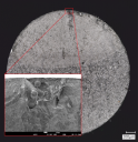
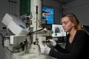
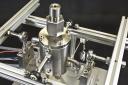
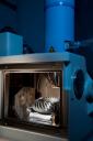
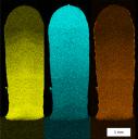
Images
| Preview | Description |
|---|---|
Source: Fraunhofer IWS |
Analytic transmission electron microscope 200 kV- JEOL JEM-2100Plus |
Last Update
Last updated at: 5 August 2019 at 10:26:56