 View all services of this unit
 Metrology and Inspection
Basic Information
| Name: | Metrology and Inspection | |
| Facility: | 200 mm MEMS-Cleanroom | |
| Partner: | Fraunhofer Institute for Photonic Microsystems (IPMS) |
|
Description
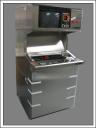
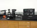
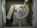
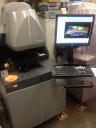
Metrology and inspection are crucial processes in semiconductor manufacturing, ensuring the accuracy and quality of wafers by measuring critical dimensions and detecting defects at various stages of processes. With our instruments we can perform thickness measurements, surface characterization, defect classification, sheet resistance and stress.
Types of Service
- This service is provided as a standard/ routine service without research activity.
- This service is provided as a research activity e.g. as a development or improvement of methods tools or within research collaborations.
Points of Contact
Associated Instruments
Last Update
Last updated at: 14 January 2025 at 14:07:38