 View all instruments of this unit
 Electron Microscopy Hitachi; Thermo Fischer; FEI Tecnai S-5000; Apreo S; F20
Basic Information
| Name: | Electron Microscopy | |
| Manufacturer: | Hitachi; Thermo Fischer; FEI Tecnai | |
| Model: | S-5000; Apreo S; F20 | |
| Facility: | Analytics and Metrology of the 300 mm CMOS Cleanroom | |
| Partner: | Fraunhofer Institute for Photonic Microsystems (IPMS) |
|
Description
Electron microscopy uses an electron beam to illuminate a specimen and create a magnified image. Two different types of electron microscopes are available: scanning electron microscopes (SEM, resolution down to ~1 nm) and transmission electron microscopes (TEM, resolution down to 0.1 nm). In SEM the electron beam is scanned over the sample and either the emitted secondary electrons or the back scattered electron are used for imaging the sample surface. In TEM the electron beam is passed through a thin lamella containing the region of interest.
At our SEM complementary element and grain analysis by means of EDX & EBSD/TKD is possible. Due to the arrangement of the attached detectors both methods can be carried out simultaneously. Where the EDX analysis unfolds the elemental composition, grain analysis gives information about the crystallographic structure & possible texture. Transmission Kikuchi diffraction (TKD) adds thereby the capability of analyzing nanostructured materials & thin films on electron-transparent lamellae, whereas EBSD analysis is carried out on larger areas on the bulk material.
The emerging beam carries information about the structure of the sample that can be evaluated in different ways. On our TEM there are six different ways we can utilize the information created by the transmission electron beam:
- Bright field imaging / Dark field imaging
- High angle annular dark-field scanning
- TEM (HAADF-STEM)
- Energy dispersive X-ray spectroscopy (EDX)
- Electron energy loss spectroscopy (EELS) and
- Energy-filtered TEM (EFTEM).
Capabilities
- Evaluation of an etching process
- Physical failure analysis
- HAADF-STEM
- EDX profiling of thin film stacks
- EBSD/TKD
- EFTEM
Tools
- Thermo Fisher Apreo S
- Hitachi S5000
- FEI Tecnai F20
Link to Further Details
Points of Contact
Dr. Nora Haufe
Web:
Phone:
+49 351 26 07-3020
Notes
This is an instrument within the Dresden Fraunhofer Cluster Nanoanalysis (DFCNA).
Associated Services
| Name | Preview | Actions |
|---|---|---|
| Analytics and Metrology |
Images
| Preview | Description |
|---|---|
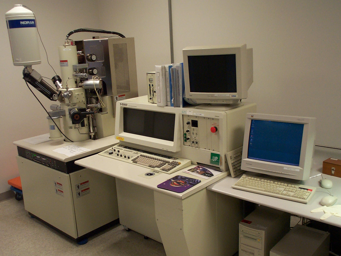
|
FE SEM Hitachi S5000 (Quelle: www.fabsurplus.com) |
Last Update
Last updated at: 20 December 2024 at 13:43:33