 View all services of this unit
 Analytics and Metrology
Basic Information
| Name: | Analytics and Metrology | |
| Facility: | 300 mm CMOS Cleanroom | |
| Partner: | Fraunhofer Institute for Photonic Microsystems (IPMS) |
|
Description
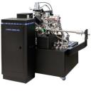
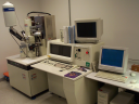
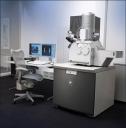
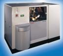
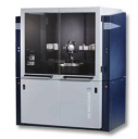
Fraunhofer IPMS offers a wide variety of analytical characterization methods in our physical failure analysis labs. We focus on wafer characterization using various X-ray methods (XPS, XRD/XRR, and TXRF), as well as Raman spectroscopy and ToF-SIMS. Furthermore, high resolution electron microscopy (SEM, TEM with EDX, EFTEM, EELS) and grain analysis (EBSD/TKD) with corresponding preparation techniques (FIB, Precision Ion Polish, Mechanical preparation) are available. Atomic and Piezoelectric force microscopy (AFM/PFM) as well as chemical etching of wafer surfaces complements the portfolio. In addition, complete electrical characterization is available here.
Our in-line metrology enables us to determine physical and chemical properties of structures on 300 mm wafers with, for example, X-ray diffraction, angle-resolved X-ray photoelectron spectroscopy, spectral ellipsometry and energy dispersive X-ray spectroscopy. All our tools for wafer level analysis are stationed in a class 1000 (class 6 ISO 14644-1) cleanroom environment that meets industrial standards.
Link to Further Details
Types of Service
- This service is provided as a standard/ routine service without research activity.
- This service is provided as a research activity e.g. as a development or improvement of methods tools or within research collaborations.
Points of Contact
Associated Instruments

Last Update
Last updated at: 15 January 2025 at 09:14:44